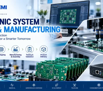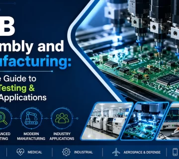
Modern electronic products are getting smaller, smarter, and more complex. A robust printed circuit board (PCB) is nearly a given in every electronic system, from automotive control systems and medical devices to industrial automation equipment, IoT products, and consumer electronics.
Traditional manual assembly methods can be difficult to scale with increasing production needs. Manufacturers need more speed, more precision, more consistency, and more quality control. This is where automated PCB manufacturing comes into play.
Automated PCB manufacturing is the use of advanced machinery and software-controlled processes and inspection systems to efficiently manufacture and assemble printed circuit boards. Technologies like Surface Mount Technology (SMT), automated pick-and-place systems, reflow soldering, 3D solder paste inspection, and Automated Optical Inspection (AOI) allow manufacturers to manage complex PCB designs and also ensure consistency in production.
Automation can provide a more structured and scalable manufacturing process for businesses looking to scale up from prototypes to high-volume production.
What Is Automated PCB Manufacturing?
Automated PCB manufacturing is the process of manufacturing, assembly, inspection, and testing of printed circuit boards (PCBs) by means of automated equipment and digitally controlled processes.
PCB manufacturing is the process of making the bare circuit board, and PCB assembly is the process of mounting electronic components on the board. These processes work together as part of a larger production workflow in a modern electronics manufacturing environment.
A typical automated PCB assembly line can consist of:
- Solder paste print
- Solder Paste Inspection (SPI)
- Automated component placement
- Reflow soldering
- Through-Hole Construction
- Automated Optical Inspection (AOI)
- X-ray inspection
- In-Circuit Testing (ICT)
- Functional Test
- PCB Panelization
- Conformal coating
The level of automation can vary depending on the product, production volume, PCB design, and required testing standards.
For example, SMT assembly uses automated pick-and-place equipment to position surface-mount components accurately on a PCB. After placement, the board passes through a controlled reflow soldering process to create reliable solder joints. Inspection and testing are then used to identify manufacturing defects.
How Does the Automated PCB Manufacturing Process Work?
An automated PCB assembly process is normally broken down into a number of specific controlled steps.
1. PCB Design and Production
Planning engineers design the PCBs and prepare the manufacturing data for manufacturing. The information needed will depend on the specific product:
- PCB layout data
- Gerber files, bill of materials (BOM)
- Pick-and-place files
- Assembly drawings
- Component specifications
- Testing requirements
Whether the design is optimised for manufacturing, i.e., Design-for-Manufacturing (DFM), is important, as this can influence manufacturing costs and timescales.
2. Solder Paste Printing
For SMT assembly, the process begins with printing the solder paste onto the PCB with a stencil printer.
The stencil contains openings corresponding to the PCB pads on the board; the printer deposits the correct amount of solder paste onto the solder pads, and the accuracy of this process can influence the quality of the final product.
Newer production lines can use 3D Solder Paste Inspection (SPI) to verify the amount of solder printed onto the board before placing components.
3. Automated Component Placement
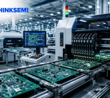
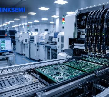
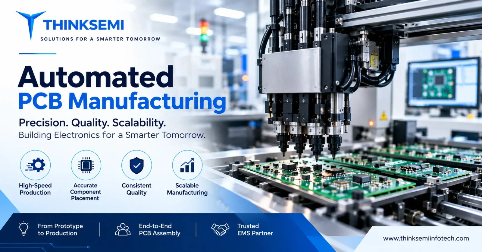
The PCB now moves into the pick-and-place machine, which automatically takes components from their feeding systems and places them onto the correctly marked locations on the PCB.
Some of the component types include
- resistors
- capacitors
- integrated circuits
- Connectors
- Microcontrollers
- sensors semiconductor devices
With high-speed pick-and-place technology, Thinksemi can place millions of components per hour, which is ideal for high-volume production.
4. Reflow Soldering
The printed circuit board then moves into a reflow oven.
which gradually heats the entire board so the solder becomes liquid and forms robust electrical connections between the component leads and PCB contacts.
As the whole process is carried out, the oven gradually cools the PCB, ensuring a solid mechanical as well as electrical connection.
It’s vital to have a carefully managed reflow profile, as some components have specific requirements.
5. Through-Hole Technology THT
There are some components that are not suitable for SMT assembly.
Especially where you want to have additional mechanical strength, through-hole components are the answer.
THT involves passing component leads through holes in the PCB and soldering them into position.
In this case, the PCB is then moved into a wave soldering machine, but only if the through-hole components are compatible with automated soldering.
6. Automated Inspection
The assembled PCB then passes through inspection with the use of either Automated Optical Inspection (AOI) or 3D SPI for inspection.
Good cameras and software algorithms will look for:
- Missing parts
- Misplaced parts
- Soldering or other assembly defects.
- Improperly configured parts.
There is a defect on the assembled PCB (Thinksemi offers AOI, 3D SPI, and other inspection technologies). If the assembly has no visible features that can be checked with optical inspection, the board may need to go through X-ray inspection.
7. Electrical and Functional Testing
The visual inspection alone cannot tell whether the PCB is functioning correctly. Depending on the product, manufacturers may run In-Circuit Testing (ICT) and/or Functional Circuit Testing (FCT) to confirm electrical performance.
This may help identify issues that cannot be visually seen. For industry-quality applications, rigorous testing is essential; otherwise, the performance of the PCB may impact the reliability of the complete electronics system.
Benefits of Automated PCB Manufacturing
Automation has proven to be advantageous for modern electronics manufacturing, especially in helping to manage the growing complexity of modern products and the volumes demanded by today’s markets.
1. Faster Manufacturing
Automated machines can insert components and assemble PCBs at much higher speeds than manual assembly processes. This allows for higher-volume production when time is tight, such as for manufacturing thousands of individual boards in a set amount of time.
Faster production can also speed the introduction of new products by shortening development cycles.
2. Higher Component Placement Accuracy
Automated pick-and-place equipment can reliably place individual components on a PCB with high precision and consistency. This is especially important for products with complex and densely populated PCBs, as well as for small-sized components.
3. Accurate and Repeatable Production
Manual PCB assembly processes can fluctuate based on operator skill and process conditions, which can impact product quality. Automation can help achieve consistency in production because each step is performed according to a set of predetermined conditions.
Integrating automated testing and inspection systems can also add further controls to maintain quality throughout production.
4. Flexibility to Scale Production
Automated equipment can also support increased production volumes and production variants. A contract manufacturing supplier might need to begin with a small initial production run of a prototype and then scale up to full production. Automated processes make it easier to adapt manufacturing systems for larger production quantities.
5. Less Human Error
Manual production inherently introduces possibilities for human error.
Although automation cannot eliminate all errors, it can decrease the incidence of errors in repetitive operations like PCB assembly by following exact placement patterns and process parameters.
Combining automation with human procedures and inspection can lead to more consistent product quality.
6. Cost Savings at High Volumes
Investing in automation equipment can cost more initially, but by streamlining production and reducing labour costs, the automation can prove more cost-effective at high volumes over time.
Hand-Soldered vs Automated PCB Manufacturing Assembly
Automated PCB Manufacturing:g Assembling PCBs by hand is often still an option for some prototypes, repairs and niche low-volume applications. This does become a challenge when production volumes rise.
| Factor | Manual Assembly | Automated PCB Manufacturing |
| Production speed | Lower | High |
| Component placement | Operator-dependent | Machine-controlled |
| High-volume production | Difficult to scale | Designed for scalability |
| Repeatability | Can vary | Highly consistent |
| Inspection | Often manual | Automated inspection available |
| Complex PCB designs | More challenging | Better suited |
| Production data | More manual | Digitally controlled |
The right manufacturing approach ultimately depends on the PCB design, production quantity, component mix, budget and quality requirements.
Applications of Automated PCB Manufacturing
Automated PCB manufacturing has applications in many industries.
Automotive and EV
Modern vehicles include many sensors, communication modules and control systems,s as well as power electronics, so reliable PCB assembly is an essential element of automotive electronics manufacturing.
Medical Electronics
Medical Electronics: As well as being used for diagnostics and monitoring, medical electronics devices are becoming more advanced and compact and demand high-reliability PCB assembly.
Industrial Automation
Industrial Automation: Industrial control systems, sensors and communications boards are an integral part of automation systems, and high-quality, cost-effective automated PCB assembly is a key enabler.
Consumer Electronics
Modern consumer electronic devices are increasingly compact and require high-density, high-reliability PCB assemblies, which is something SMT automation can provide.
IoT and Smart Devices
IoT and Smart Devices: As IoT devices can require densely populated PCBs as well as highly integrated systems based on high-density sensor arrays and processors, high-quality automated PCB assembly is an important manufacturing process.
Aerospace and Defence
Aerospace and Defence: Aerospace and defence electronics often have to meet rigorous requirements for reliability and include complex assembled components that require suitable inspection and testing regimes. About Thinksemi offers EMS and PCB assembly services for many industries, including automotive, medical, industrial, consumer electronics, aerospace, defence, IoT, EV and telecoms.
Selecting Your Automated PCB Manufacturing Partner
Selecting an automated manufacturing partner is not just about a comparison of how many PCBs can be produced each day.
Other considerations include:
Manufacturing Capabilities
Ensure that the manufacturer can support the PCB technologies you require, such as THT, THT and mixed-technology assembly, and complex PCB stacks.
Inspection and Testing
Inquire about inspection and testing procedures, such as SPI, AOI, X-ray, ICT, and functional testing.
Scalability
Your manufacturing partner should be able to support the product beyond the prototype phase and scale production as needed.
Component Sourcing
Component procurement has a significant role to play in PCB manufacturing. Supply chain management can determine how quickly PCBs are manufactured, component availability, and project costs.
Quality Certifications
Any information about the quality management system at the manufacturer can be gleaned from its certifications. Thinksemi states that it is IATF 16949 and ISO 9001:2015 certified.
End-to-End Services
Partnering with a manufacturer capable of providing multiple stages of the manufacturing process can help simplify supplier management. Thinksemi’s capabilities include PCB assembly, PCB prototyping, component sourcing, testing, box build assembly, wiring harness assembly, and product engineering/ODM.
Automated PCB Manufacturing at Thinksemi Infotech
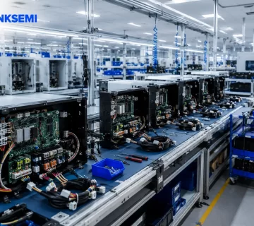
Thinksemi Infotech delivers electronic manufacturing services and PCB assembly for customers looking for prototype and production manufacturing. Its manufacturing plant is located at SIPCOT IT Park, Siruseri, Chennai, and the company states that the plant has ESD-safe standards and is equipped with automated manufacturing and inspection systems. Its capabilities include SMT, wave soldering, AOI, 3D SPI, ICT, PCB depanelisation, and conformal coating.
The company also offers PCB prototyping, component sourcing, testing, box build assembly and other electronic manufacturing services, providing for customers across a variety of sectors.
Getting from prototype to production is easier when working with an integrated electronics manufacturing partner who can take care of manufacturing, sourcing, assembly, testing and product integration.
Conclusion
Automated PCB manufacturing is now a key component of modern-day electronic product manufacturing. As electronic products become more miniaturised, connected, and complex, manufacturers require production methods that are accurate, repeatable, and fast.
From printing solder paste to placement and reflow soldering to inspection and functional testing, automation can optimise many PCB assembly steps.
For the customer, the aim is not just to produce more PCBs but to establish a controlled and scalable process capable of reliably manufacturing high-quality PCB assemblies.
With the right automated manufacturing systems, PCB assembly and engineering teams, quality assurance procedures, and testing processes, the transition from prototype to full production can be well managed by the electronics manufacturing partner.